1. סקירת מוצר:
למרות שהם דומים מבחינה מבנית למסנני חלל עם דחייה מחוץ לפס העולה על 60dB, מסנני הסרט הדק המיניאטורי שלנו משיגים את אותם ביצועים תוך שהם תופסים רק 1/500 מהנפח ומשקלם רק 1/350 ממסנני חלל קונבנציונליים.
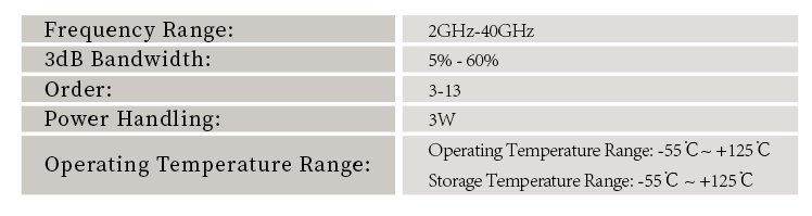
2. מאפייני ביצועים חשמליים:
3. הוראות הרכבה והפעלה
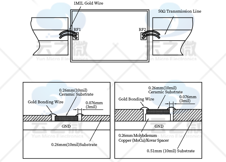
1) מסנן הסרט הדק הוא רכיב פסיבי מיניאטורי עם ממשקי קלט/פלט RF הניתנים להחלפה. במהלך ההתקנה, נדרש בידוד חלל: יש לשמור על מרווח מינימלי של 3 מ"מ בין המשטח העליון של המסנן לבין כיסוי המגן המתכתי, עם מרווח של כ-0.2 מ"מ בין דופן הצד של המסנן לחלל.
2) יש להרכיב את המסנן על גבי מצע נשא בעל מקדמי התפשטות תרמיים תואמים, כגון קובאר (מומלץ) או סגסוגות מוליבדן-נחושת. עובי הנשא צריך להיות ≥0.3 מ"מ (מומלץ 0.5 מ"מ).
3) להרכבה על משטח תחתון, יש למרוח כמות מתאימה של דבק מוליך (מומלץ ME8456 או EG8050) כדי להבטיח הארקה תקינה תוך הימנעות מזיהום מוגזם של קווי תמסורת RF.

כתובת : Xisan Road, Mechanical and Electrical Industrial Park, No.767 Yulan Road, Hefei,Anhui.
טל : +86-18855146875
אימייל : liyong@blmicrowave.com


לסרוק אותו